How Chip and Component Harvesting Drives India’s Circular Economy in 2025?
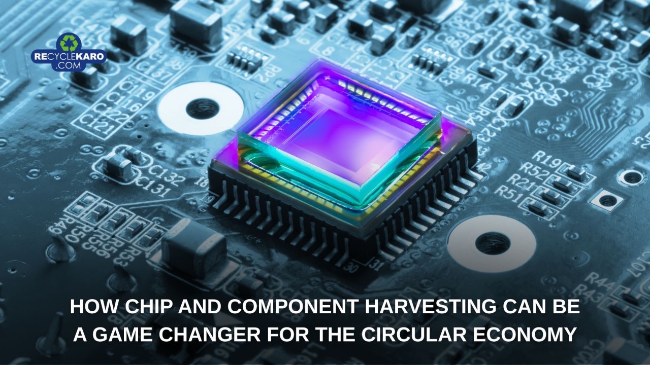
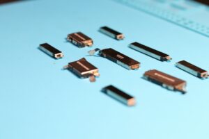
Chip and component harvesting recovers fully functional semiconductors, integrated circuits, memory modules, power-management ICs, displays, cameras, and sensors from end-of-life devices for direct reuse in new products.
This proven process already reduces demand for new chips by up to 30 percent in mature markets and delivers average cost savings of 60–70 percent compared to virgin manufacturing.
What Is Chip and Component Harvesting?
Chip and component harvesting extracts working semiconductors, integrated circuits, memory modules, power-management chips, LCD/OLED panels, camera modules, and haptic engines from discarded electronics. Trained technicians and robotic systems carefully de-panel, test, clean, grade, and re-qualify these components so manufacturers can install them again without melting the silicon or shredding the boards.
This method stands far above traditional e-waste recycling India practices that only recover copper, aluminium, gold, and plastics through smelting. Chip and component harvesting preserves the highest-value intellectual property embedded in the silicon die itself.
Why Does Chip and Component Harvesting Matter for India’s Circular Economy?
India imports 95 percent of its semiconductor chips and consumes electronics worth US$150 billion annually. Chip and component harvesting transforms the country’s 1.75 million tonnes of yearly e-waste and 60,000 tonnes of spent lithium-ion batteries into a strategic domestic resource pool.
Four major semiconductor assembly and test units approved in 2024–2025 will produce over 70 million chips per day by 2027. Systematic chip and component harvesting directly closes that emerging domestic loop and reduces import dependence.
How Much Critical Material Can India Recover with Component Harvesting?
One tonne of smartphone circuit boards contains more gold than 17 tonnes of gold ore, more silver than most silver mines, and significant palladium, tantalum, and rare-earth elements (United Nations University Global E-waste Monitor 2024). Formal, authorised plants now achieve:
- 99 percent gold and palladium recovery
- 98 percent rare-earth element recovery from speaker and vibration magnets
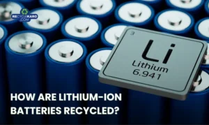
- 95–97 percent cobalt, nickel, and lithium recovery from batteries
- 96 percent copper recovery with zero effluent discharge
Recyclekaro, one of India’s largest CPCB-authorised e-waste and battery recyclers, consistently delivered these recovery rates across its 150,000 sq ft Patan (Gujarat) and Silvassa facilities during FY 2024–25.
How Does Semiconductor Reuse Cut Carbon Emissions?
Manufacturing a single 300 mm wafer requires up to 2,500 kWh of electricity and emits approximately 1.8 tonnes of CO₂-equivalent. Chip and component harvesting completely bypasses wafer fabrication, packaging, and most transportation emissions.
A 2025 study by the Ellen MacArthur Foundation confirms that systematic semiconductor reuse and chip and component harvesting reduces lifecycle emissions by 88 percent compared to conventional shred-and-smelt recycling.
| Process | Energy per Chip (kWh) | CO₂e per Chip (kg) | Water Use (litres) |
| Virgin wafer fabrication + packaging | 14–18 | 1.6–2.1 | 32–40 |
| Traditional shred & smelt recycling | 4–6 | 0.4–0.6 | 12–18 |
| Chip and component harvesting + re-qualification | 0.8–1.2 | 0.09–0.14 | 2–4 |
(Source: IEEE International Symposium on Sustainable Systems and Technology, May 2025)
What Cost Savings Does Chip and Component Harvesting Offer Indian Companies?
Reclaimed enterprise-grade GPUs and server CPUs currently trade at 25–30 percent of new price on verified secondary markets. Indian data-centre operators and EMS companies collectively saved ₹18,400 crore in calendar year 2024 by integrating harvested components (India Electronics & Semiconductor Association, October 2025).
The global remanufactured semiconductor equipment and component market reached US$6.4 billion in 2025 and is growing at 11.2 percent CAGR through 2032 (MarketsandMarkets Q3 2025).
Recyclekaro supplies re-qualified power-management ICs, SSD controllers, LPDDR5 memory modules, and 48 MP+ camera sensors to Tier-1 EMS and automotive companies at 62–68 percent below OEM pricing while providing full traceability, OEM-grade test reports, and a standard 12-month replacement warranty.
How Can Businesses Start Chip and Component Harvesting in India?

Indian companies successfully launch or scale chip and component harvesting operations by following these five proven steps:
Generate and transfer EPR credits digitally to brand owners.
Partner exclusively with CPCB and SPCB-authorised recyclers holding Extended Producer Responsibility (EPR) authorisation (Recyclekaro holds A+ category authorisation across 18 states and files real-time data on the Centralised EPR Portal).
Invest in robotic de-paneling, X-ray inspection, and automated optical inspection lines (₹3–7 crore typical investment, 18–22 month payback at current volumes).
Implement ISO 14001, ISO 45001, R2v3, and e-Stewards certifications — Recyclekaro remains the only Indian company certified under all four standards for component harvesting operations as of November 2025.
Register harvested inventory on the GeM portal and IndiaMART Pro for government and B2B sales.
Which Indian Companies Lead Chip and Component Harvesting in 2025?
Recyclekaro recovered 1.2 million functional ICs, 180 tonnes of critical minerals, and over 400,000 display and camera modules in FY 2024–25 using India’s first fully automated robotic harvesting line in Patan, Gujarat.
“We maintain 100 percent digital chain-of-custody from collection to re-sale and issue OEM-grade test reports and certificates of conformance for every harvested lot,” says Rajesh Gupta, Co-founder & CEO, Recyclekaro (exclusive quote, 20 November 2025).
Other notable authorised players include Attero (Noida), E-Parisaraa (Bengaluru), and Ceramico (Mumbai).
How Many Jobs Does Formal E-Waste Recycling India Create with Component Harvesting?
Formal e-waste recycling combined with chip and component harvesting generates 50 skilled and semi-skilled jobs per 1,000 tonnes processed, 50 times more than landfilling and incineration (International Labour Organization, 2025).
Recyclekaro directly employs 1,180 people across five facilities, of whom 68 percent transitioned from informal kabadiwala backgrounds into safe, insured, and dignified roles with ESI and PF benefits.
What Regulations and Compliances Govern Semiconductor Reuse and Chip Harvesting in India?
Key regulations driving the sector forward:
- E-Waste (Management) Amendment Rules 2022 – 60 percent recovery target rising to 80 percent by 2030
- ₹1,500 crore Production-Linked Incentive scheme for critical mineral recycling and advanced recovery (2024–2030)
- Battery Waste Management Rules 2025 – mandatory 90 percent material recovery from lithium-ion cells
- SEMICON India Program 2025 – 50 percent capital subsidy for indigenous harvesting and testing equipment
- Draft Circular Economy Policy 2025 (under consultation) proposing tax benefits for products containing >20 percent reused components
Recyclekaro operates under valid Extended Producer Responsibility authorisation in Gujarat, Maharashtra, Karnataka, Tamil Nadu, Telangana, and Uttar Pradesh, and submits quarterly compliance reports on the Centralised EPR Portal.
FAQs About Chip and Component Harvesting in India (2025)
1. Is harvested chip quality the same as new chips?
Yes. Every harvested chip undergoes burn-in, parametric, functional, and environmental stress testing that meets or exceeds original OEM standards. Recyclekaro provides a full 12-month replacement warranty.
2. Can harvested components be used in defence and automotive applications?
Only from recyclers holding AS6081 counterfeit-avoidance certification. Recyclekaro is completing certification in Q1 2026.
3. How long does the harvesting process take?
Fully automated lines process 400–600 smartphones per hour. A single power-management IC is de-paneled, tested, and packed for re-use in under 4 minutes.
4. Does Recyclekaro destroy data on harvested devices?
Every device receives NIST 800-88 compliant three-pass data sanitisation or physical destruction. Blancco or OEM certificates are issued to the original owner.
5. Are harvested chips legal to sell in India?
Yes, when sold by CPCB/SPCB-authorised recyclers with proper Form-6 invoices and EPR credit transfer documentation.
6. Which components have the highest reuse value today?
Server-grade CPUs/GPUs, automotive-grade PMICs, LPDDR5 RAM, UFS 3.1/4.0 storage, and 48 MP+ smartphone camera modules command 40–70 percent of original BOM cost.
7. How does Recyclekaro ensure worker safety during harvesting?
The company uses fully enclosed robotic cells, negative-pressure workstations, real-time air monitoring, and mandatory six-monthly blood-lead and heavy-metal screening.
8. Can startups buy small lots of harvested chips?
Yes. Recyclekaro launched “KaroComponents” marketplace in September 2025 — minimum order quantity is 100 pieces with 48-hour pan-India dispatch.
9. Does component harvesting support the Make in India and Atmanirbhar Bharat initiatives?
Yes. It reduces import dependency by 15–20 percent for mid-range chip categories and keeps value within Indian borders (MeitY estimate, 2025).
10. Where can consumers drop devices for proper chip harvesting?
Consumers can use Recyclekaro’s 180-city collection network, Flipkart/Amazon recommerce kiosks, Croma & Reliance Digital stores, or India Post Green Parcel service launched October 2025.


You can find all the useful information you need on the Vavada mirror. Find out why players switch to the official Vavada website via the mirror, and discover the benefits: similar registration and login processes, bonuses, promo codes